Introduction
In the ever-evolving world of digital electronics, the Programmable Logic Array (PLA) remains a foundational component for designing custom logic circuits. As the first Programmable Logic Device (PLD), PLAs revolutionized how engineers approach circuit design by offering flexibility and efficiency. This guide dives deep into PLAs, their structure, applications, and relevance in 2025. Whether you’re a student, hobbyist, or professional, this article simplifies complex concepts into easy-to-understand language.
What is a Programmable Logic Array (PLA)?
A PLA is a type of PLD that uses a matrix of programmable AND and OR gates to implement custom logic functions. Unlike fixed-function ICs, PLAs allow users to configure their internal connections (via fusible links) to match specific application needs. This makes them ideal for prototyping and optimizing circuits without redesigning hardware.
Key Features of PLA:
- Dual Programmability: Both AND and OR arrays can be customized.
- Cost-Effective: Reduces the need for multiple discrete components.
- Reusable: Can be reprogrammed for different logic functions.
Block Diagram of PLA
Let’s break down the PLA’s architecture using its block diagram:
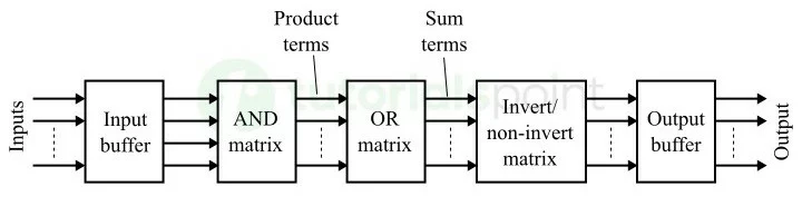
1. Input Buffer
The input buffer prevents loading effects, ensuring the input source isn’t overwhelmed by the PLA’s internal circuitry.
2. AND Matrix
This array generates product terms (AND operations) from input signals. Each row represents a unique combination of inputs.
3. OR Matrix
The OR matrix combines product terms into sum terms, producing the final output logic.
4. Invert/Non-Invert Matrix
This buffer sets outputs as active-high or active-low, adding flexibility to match downstream components.
5. Output Buffer
Boosts the signal strength to drive external devices efficiently.
Combinational Logic Design Using PLA
PLAs excel in designing combinational circuits. Here’s a step-by-step approach:
Step 1: Create a PLA Program Table
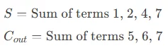
List inputs, product terms, and outputs. For example, a full-adder circuit with inputs A, B, Cin and outputs S (sum) and Cout (carry).
Step 2: Design the AND Matrix
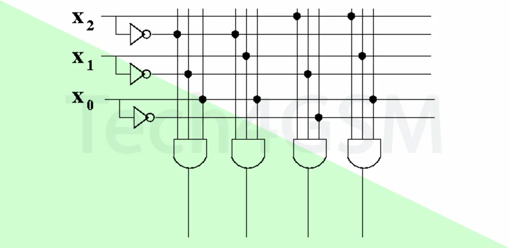
Map input combinations to product terms. The full-adder requires 7 product terms:
Step 3: Design the OR Matrix
Combine product terms for outputs:
Step 4: Configure Invert/Non-Invert Matrix
Set outputs to active-high (T) or active-low (F).
Step 5: Program the PLA
Burn fusible links based on the program table to finalize the circuit.
Example: Designing a Full-Adder with PLA
Let’s apply the above steps to create a full-adder:
Truth Table for Full-Adder
| A | B | Cin | S (Sum) | Cout (Carry) |
|---|---|---|---|---|
| 0 | 0 | 0 | 0 | 0 |
| 0 | 0 | 1 | 1 | 0 |
| 0 | 1 | 0 | 1 | 0 |
| 0 | 1 | 1 | 0 | 1 |
| 1 | 0 | 0 | 1 | 0 |
| 1 | 0 | 1 | 0 | 1 |
| 1 | 1 | 0 | 0 | 1 |
| 1 | 1 | 1 | 1 | 1 |
Explanation
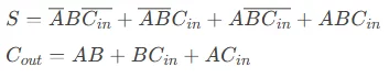
- Sum (S): Represents the XOR of A, B, and Cin. It is 1 when an odd number of inputs are 1.
- Carry (Cout): Becomes 1 when two or more inputs are 1, indicating a carry to the next higher bit.
Boolean Expressions:
PLA Program Table for Full-Adder
| Sr.No | Product Terms | Inputs | Outputs | |||
|---|---|---|---|---|---|---|
| A | B | C<sub>in</sub> | S | C<sub>out</sub> | ||
| 1 | A‾BCin‾ | 0 | 1 | 0 | 1 | – |
| 2 | A‾B‾Cin | 0 | 0 | 1 | 1 | – |
| 3 | AB‾Cin‾ | 1 | 0 | 0 | 1 | – |
| 4 | ABCin | 1 | 1 | 1 | 1 | 1 |
| 5 | AB | 1 | 1 | – | – | 1 |
| 6 | BCin | – | 1 | 1 | – | 1 |
| 7 | ACin | 1 | – | 1 | – | 1 |
Key Notes:
- Inputs:
- 0: Input is complemented (A‾, B‾, etc.).
- 1: Input is true (A, B, etc.).
- –: Input is ignored (don’t care).
- Outputs:
- 1: Product term contributes to the output.
- –: Product term does NOT contribute to the output.
- Shared Term (Row 4):
- The term ABCin is used for both Sum (S) and Carry (C<sub>out</sub>).
- Design Workflow:
- AND Matrix: Burns fusible links for the product terms above.
- OR Matrix: Combines terms for S (rows 1–4) and Cout (rows 4–7).
Circuit Diagram:
Advantages of PLAs
- Flexibility: Reconfigure for multiple logic functions.
- Cost Savings: Eliminates need for discrete gates.
- Time Efficiency: Faster prototyping compared to custom ICs.
- Compact Design: Integrates complex logic into a single chip.
Disadvantages of PLAs
- Complexity: Scaling up inputs/outputs increases design difficulty.
- Speed Limitations: Fixed architecture may lag behind ASICs.
- Power Consumption: Higher than dedicated ICs for simple tasks.
Applications of PLAs in 2025
- IoT Devices: Custom logic for sensor data processing.
- AI Hardware: Implementing lightweight neural networks.
- Automotive Systems: Control logic for EVs and autonomous driving.
- Consumer Electronics: Used in smart home gadgets.
- Telecom: Signal routing and error correction in 5G/6G systems.
FAQs About PLAs
Q1: How is PLA different from FPGA?
A: PLAs have fixed AND/OR arrays, while FPGAs offer more granular programmability with lookup tables and interconnects.
Q2: Can PLAs handle sequential circuits?
A: Basic PLAs are combinational, but some variants include flip-flops for sequential logic.
Q3: Are PLAs obsolete in 2025?
A: No! They’re still used in cost-sensitive, low-complexity applications.
Q4: What tools program PLAs?
A: Hardware description languages (HDLs) like VHDL or dedicated software from manufacturers.
Conclusion
The Programmable Logic Array (PLA) continues to be a vital tool in digital design, balancing simplicity and adaptability. As we move into 2025, its role in IoT, AI, and telecom underscores its enduring relevance.