Introduction
A Printed Circuit Board (PCB) is the backbone of almost every electronic device you use today. Imagine it as a city map where electronic components like resistors, capacitors, and microchips are the buildings, and the copper traces are the roads connecting them. This “map” ensures electricity flows smoothly, allowing your smartphone, laptop, or even your car’s GPS to function.
PCBs are made from non-conductive materials like fiberglass (rigid PCBs) or flexible plastics (flexible PCBs), layered with conductive copper pathways. Over the years, PCBs have evolved from simple single-layer designs to complex multi-layered structures, enabling advancements in technology like foldable phones and wearable health monitors. By 2025, experts predict even smaller, faster, and eco-friendly PCBs will dominate industries.
A Brief History of PCBs
The first PCBs appeared in the 1940s, using bulky wires and manual assembly. By the 1980s, surface-mount technology (SMT) revolutionized PCB manufacturing, allowing smaller components and automated production. Fast forward to 2025, innovations like 3D-printed PCBs and biodegradable materials are set to redefine electronics.
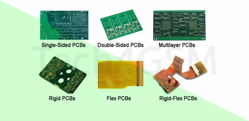
Types of PCBs: Which One Fits Your Needs?
- Single-Layer PCBs:
- The simplest and cheapest type.
- Used in calculators, LED lights, and basic toys.
- Components are mounted on one side, with copper traces on the other.
- Double-Layer PCBs:
- Copper layers on both sides, connected by “vias” (tiny holes).
- Ideal for automotive dashboards and power converters.
- Multi-Layer PCBs (4 to 12+ layers):
- Used in smartphones, medical devices, and aerospace tech.
- Layers alternate between conductive and insulating materials for high-speed performance.
- Flexible PCBs:
- Made from bendable plastics.
- Perfect for smartwatches, foldable phones, and curved TVs.
- Rigid-Flex PCBs:
- Combine rigid and flexible layers.
- Common in drones, military gear, and advanced robotics.
PCB Layers Explained: What’s Inside Your Circuit Board?
Every PCB is a sandwich of specialized layers:
- Substrate (Base Layer):
- Usually made of FR-4 (fiberglass and epoxy) for rigidity.
- Flexible PCBs use polyimide to withstand bending and high temperatures.
- Conductive Layer (Copper Traces):
- Thin copper sheets etched into pathways.
- Double-layer PCBs have copper on both sides.
- Solder Mask (The Green Coat):
- Insulates copper traces to prevent short circuits.
- Available in colors like red, blue, or black for branding.
- Silkscreen (Labels):
- White text indicating component placement (e.g., “R1” for Resistor 1).
Key PCB Components and Their Roles
- Resistors: Control electricity flow like a water valve.
- Capacitors: Store and release energy, like a battery.
- Diodes: One-way streets for current.
- Transistors: Amplify signals or act as switches.
- Sensors: Detect heat, light, or motion (e.g., your phone’s fingerprint scanner).
Through-Hole vs. Surface-Mount Components:
- Through-hole parts (older tech) are sturdy but bulky.
- Surface-mount (SMT) components are tiny, allowing sleeker designs like modern laptops.
Where Are PCBs Used? Applications in 2025
- Consumer Electronics: Smartphones, gaming consoles, and IoT devices like smart fridges.
- Healthcare: MRI machines, pacemakers, and wearable glucose monitors.
- Automotive: Electric car batteries, infotainment systems, and self-driving sensors.
- Aerospace: Navigation systems and satellite communication.
By 2025, expect PCBs in AI-powered robots, solar-powered IoT devices, and brain-computer interfaces!
How Are PCBs Made? A Step-by-Step Guide
- Design: Engineers use software like AutoCAD to create blueprints.
- Printing: A printer transfers the design onto the substrate.
- Etching: Chemicals remove excess copper, leaving only traces.
- Drilling: Lasers create holes for vias and components.
- Assembly: Robots place components.
- Testing: PCBs undergo rigorous quality checks.
Future Trends in PCB Technology (2025 and Beyond)
- 3D-Printed PCBs: Faster prototyping and custom designs.
- Eco-Friendly Materials: Biodegradable substrates to reduce e-waste.
- HDI (High-Density Interconnect): More components in smaller spaces.
- AI Integration: Self-diagnosing PCBs that fix errors automatically.
FAQs About PCBs
1. What’s the difference between single-layer and multi-layer PCBs?
Single-layer PCBs have one conductive layer, while multi-layer PCBs stack multiple layers for complex tasks like data processing.
2. Can I repair a damaged PCB at home?
Yes! Simple fixes like replacing a burnt resistor are possible.
3. Are flexible PCBs durable?
Yes! They can bend thousands of times without breaking, ideal for foldable devices.
4. How long does PCB manufacturing take?
Prototypes take 3–5 days. Bulk orders may require weeks.
5. What’s the lifespan of a PCB?
Typically 20–50 years, depending on usage and environment.
6. Why are most PCBs green?
The solder mask’s default color is green, but brands use blue or black for style.
7. Can PCBs be recycled?
Yes! Copper and gold can be extracted from old PCBs.
8. What is HDI technology?
High-Density Interconnect allows ultra-thin traces, used in 5G phones and mini drones.
9. How do I choose a PCB type for my project?
Consider space, budget, and complexity. Start with single-layer for simple projects.
10. What’s next for PCBs in 2025?
Smaller sizes, faster speeds, and integration with renewable energy systems!
Conclusion
From powering your smartphone to enabling Mars rovers, PCBs are the unsung heroes of modern tech. As we approach 2025, innovations like AI-driven designs and eco-friendly materials promise to make electronics smarter and greener. Whether you’re a hobbyist or a pro, understanding PCBs opens doors to endless possibilities.