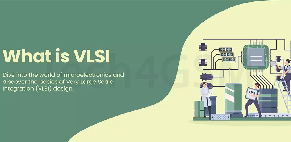
Introduction
The full form of VLSI is Very Large-Scale Integration, a technology that integrates millions of transistors onto a single microchip. This process enables the creation of compact, powerful electronic devices like smartphones, laptops, and AI systems.
How VLSI Works
VLSI combines design, fabrication, and testing to produce advanced integrated circuits (ICs). By packing countless transistors into tiny chips, VLSI reduces device size while boosting performance. For example, modern microprocessors use VLSI to deliver lightning-fast computing in devices as small as a smartwatch.
Key VLSI Design Techniques
Designing VLSI chips requires precision. Here are 7 best practices used by engineers:
- Modularity: Break designs into reusable modules for easier testing.
- Hierarchy: Organize circuits into layers (like building blocks).
- Simulation Tools: Check for errors before manufacturing.
- Power Management: Optimize energy use to extend battery life.
- Timing Closure: Ensure signals move fast enough to avoid delays.
- Design for Testing (DFT): Add features to simplify chip testing.
- 3D Integration: Stack components vertically to save space.
Why does this matter? These techniques help create smaller, faster, and cheaper chips for everyday gadgets.
VLSI’s Impact on Modern Tech
From AI to IoT, VLSI drives innovation:
- Computers: Enables high-speed processors for gaming and data centers.
- Smartphones: Powers compact, energy-efficient chips for 5G and cameras.
- IoT Devices: Lets sensors and wearables operate on minimal power.
- AI/ML: Specialized VLSI chips (like Google’s TPUs) accelerate machine learning tasks.
By 2025, VLSI will play a bigger role in self-driving cars and medical devices, thanks to its ability to handle complex computations.
VLSI in IoT and Embedded Systems
IoT devices rely on VLSI for:
- Miniaturization: Fit more features into tiny gadgets (e.g., smart thermostats).
- Low Power Use: Enable years of battery life in sensors.
- Cost Reduction: Mass production lowers prices for consumer tech.
Example: A fitness tracker uses VLSI to monitor heart rate, GPS, and Bluetooth in one chip.
VLSI Fabrication: How Chips Are Made
The process involves:
- Photolithography: Etching circuits onto silicon wafers.
- Doping: Adding chemicals to enhance conductivity.
- CMOS Technology: Most common method for energy-efficient chips.
New materials like gallium nitride (GaN) are making chips faster and more heat-resistant.
Challenges in VLSI Design
- Heat Management: Dense chips overheat easily.
- Solution: Use heat sinks and advanced cooling systems.
- Security Risks: Hackers can exploit chip vulnerabilities.
- Solution: Add encryption and secure boot mechanisms.
- Testing Complexity: Billions of transistors are hard to check.
- Solution: Built-in self-test (BIST) circuits.
Future Trends in VLSI (2025 and Beyond)
- AI-Driven Design: Automation tools to speed up chip creation.
- Quantum Integration: Merging quantum computing with VLSI.
- Eco-Friendly Chips: Reducing energy use in data centers.
VLSI Full Form in Different Languages
- Hindi: बड़े पैमाने पर एकीकरण
- Tamil: மிகப் பெரிய அளவிலான ஒருங்கிணைப்பு
- Telugu: వెరీ లార్జ్ స్కేల్ ఇంటిగ్రేషన్
FAQs
Q1. What is the full form of VLSI?
A: Very Large-Scale Integration.
Q2. How does VLSI benefit IoT devices?
A: It reduces size, power use, and cost, making IoT gadgets efficient and affordable.
Q3. What’s the future of VLSI?
A: By 2025, expect smarter AI chips, 3D designs, and greener tech.
Q4. Why is VLSI important for AI?
A: It creates specialized processors that handle AI tasks faster than standard chips.
Q5. How are VLSI chips tested?
A: Using simulations, built-in tests, and advanced tools like automatic test pattern generation (ATPG).